Talk to us

 Send Inquiry
New energy photovoltaic inverter development PCB electronic assembly
MOQ : 100 Pieces
New energy photovoltaic inverter development PCB electronic assembly Specification
- Processor Speed
- 32-bit microcontroller, 72 MHz
- Input
- DC input from solar panels (24V/48V)
- Output
- AC output (220V/230V, single phase)
- Response Time
- <30 ms (MPPT adjustment)
- Usage
- Photovoltaic inverter development and testing
- Sensors Specification
- Current/Voltage sensing via shunt resistors and optocoupler feedback
- Thermal Conductivity
- Standard FR-4 PCB, 0.25 W/m-K
- Interface
- Input/Output screw terminals
- Power Supply
- Photovoltaic (solar panel) input
- Power Source
- Photovoltaic (solar) panel powered
- Operating Temperature
- -20C to +60C
- IP Rating
- IP20 (indoor use only)
- Features
- Integrated MPPT, over-voltage protection, overcurrent protection, relay-controlled output
- Charging Voltage
- N/A (not for battery charging)
- Components
- MOSFETs, IGBTs, capacitors, transformers, microcontroller, relays
- Product Type
- Photovoltaic Inverter PCB Assembly
- Application
- Solar energy, renewable power systems, lab R&D
- Rated Voltage
- DC 24V/48V input, AC 220V/230V output
- Supply Voltage
- DC 24V/48V
- Size
- Standard PCB size, approx. 180mm x 130mm
- Dimension (L*W*H)
- 180mm x 130mm x 28mm
- Function
- DC to AC conversion for photovoltaic energy systems
- Color
- Green (PCB), multi-colored components
- Weight
- Approx. 350g
- Capacity
- Up to 1000W (depending on module configuration)
- Current Rating
- Up to 12A DC input
- Thickness
- 1.6 mm (PCB)
- Frequency
- 50Hz/60Hz AC output
- Cooling
- Provision for external fan
- Number of Layers
- 2
- PCB Finish
- HASL (Hot Air Solder Leveling)
- Mounting Type
- Through-hole and SMD mixed technology
- Communication
- UART header for firmware flashing/debug
- PCB Material
- Glass fiber FR-4
- Insulation Voltage
- 1500V AC
- ESD Protection
- Integrated on sensitive input lines
- Surge Protection
- Yes, MOVs (Metal Oxide Varistors) integrated
- Lifecycle
- Designed for R&D and prototyping applications
- Connector Type
- Screw terminal blocks for power connections
- Control Method
- Microcontroller-based PWM control
- Assembly Type
- Full electronic assembly with test points
New energy photovoltaic inverter development PCB electronic assembly Trade Information
- Minimum Order Quantity
- 100 Pieces
- Supply Ability
- 1000 Pieces Per Month
- Delivery Time
- 7 Days
About New energy photovoltaic inverter development PCB electronic assembly
Experience exceptional savings and reliable performance with our New Energy Photovoltaic Inverter Development PCB Electronic Assembly. Crafted with gorgeous, rarefied glass fiber FR-4 and remarked for its advanced microcontroller-based PWM control, this PCB assembly is optimized for R&D and prototyping in renewable energy systems. Featuring integrated surge and ESD protection, MPPT, robust MOSFETs/IGBTs, and convenient screw terminal blocks, this inverter PCB ensures seamless DC-to-AC conversion for solar panels. Reserve yours to unlock innovation-shop now and elevate your renewable energy projects!
Versatile Application and Usage
The New Energy Photovoltaic Inverter Development PCB Electronic Assembly boasts a wide surface of application, from laboratory research and development to real-world renewable energy installations. Used by engineers, researchers, and developers, it is ideal for prototyping, performance testing, and solar energy system integration. Its through-hole and SMD mixed technology, rapid response MPPT, and robust protection features make it the preferred choice for manufacturers, importers, and service providers in the energy industry.
Shipment Details and Payment Information
Shipments are processed promptly with standard rates and charges depending on destination and order quantity. Delivery time ranges from 7-15 business days post-payment. Accepted payment terms include T/T, L/C, and PayPal to accommodate diverse customers. FOB Port is typically Shanghai, China, ensuring reliable international logistics. Track your order status efficiently and rely on our dedicated support for all shipment inquiries-experience dependable service from order placement to final delivery.
FAQ's of New energy photovoltaic inverter development PCB electronic assembly:
Q: How does the inverter PCB assembly benefit photovoltaic system development?
A: The inverter PCB assembly offers integrated MPPT, reliable surge and ESD protection, and streamlined control-features that remarkably improve efficiency, safety, and ease of system prototyping and testing.Q: What is the process for reserving or ordering this inverter PCB electronic assembly?
A: To reserve or purchase, simply contact our sales team or visit our official distributor site. Proceed with the preferred payment and confirm shipment details for prompt order handling.Q: Where can the inverter development PCB electronic assembly be applied?
A: It is suitable for use in laboratory research environments, renewable energy trials, prototyping, and solar energy integration projects, making it versatile for dealers, manufacturers, and system integrators.Q: What are the main usage scenarios for this PCB assembly?
A: This PCB assembly supports DC-to-AC conversion for new energy (solar) applications, R&D prototyping, and testing of photovoltaic inverter systems.Q: How does the integrated protection system work in this PCB?
A: The assembly incorporates MOVs for surge protection and ESD safeguards on sensitive inputs. It actively shields circuits against voltage spikes, static, and overcurrent, ensuring longevity and reliability.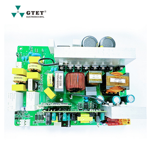
Tell us about your requirement

Price:
Quantity
Select Unit
- 50
- 100
- 200
- 250
- 500
- 1000+
Additional detail
Mobile number
Email

More Products in PCBA Modules Category
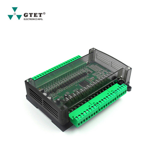
PCBA Scheme Board Development Design Industrial Control Board SMT SMD foundry vacuum reflow welding
Minimum Order Quantity : 100 Pieces
Input : Digital/Analog Signal Input
Dimension (L*W*H) : Customizable
Weight : Custom (depends on configuration and board size)
Application : Automation, process control, industrial environments, custom electronics projects
Processor Speed : Depends on microcontroller/processor selected
Medical electronic PCBA solution design laser treatment instrument control board custom development SMT patch assembly
Minimum Order Quantity : 100 Pieces
Input : Digital/analog sensor signals; user interface commands
Dimension (L*W*H) : 110mm x 80mm x 1.6mm (sample standard, customizable)
Weight : Approx. 45g (bare PCBA)
Application : Laser physiotherapy, beauty medical apparatus
Processor Speed : 32MHz (standard MCU)

Raspberry Pi industrial board board odm motherboard development SMT patch full process PCB electronic assembly processing
Minimum Order Quantity : 100 Pieces
Input : GPIO, USB, Ethernet, HDMI
Dimension (L*W*H) : 85mm x 56mm x 15mm
Weight : 55g (typical, varies by configuration)
Application : Robotics, industrial control, IoT, education, smart terminals
Processor Speed : 1.2 GHz 1.5 GHz (customizable)
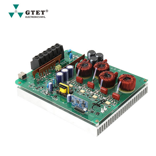
Custom solar photovoltaic control board PCBA assembly smt patch processing source scheme board development
Minimum Order Quantity : 10 Pieces
Input : PV panel DC input, sensor and data inputs.
Dimension (L*W*H) : As per customization (e.g., 100mm x 70mm x 25mm).
Weight : Approx. 100g 250g (depending on configuration).
Application : Solar photovoltaic installations, offgrid solar plants, hybrid energy storage systems.
Processor Speed : Up to 72MHz (based on microcontroller chosen).
Shenzhen Dasonghe Trading Co., Ltd.


Mr. Mike
(Manager)
Mobile : +8619926488141
8B30, Building 4, A-D& 7-15, SEG Tech Park, No. 3012, Huaqiang North Road, Futian,Shenzhen - 518000, Guangdong, China

Quick Link
Developed and Managed by Infocom Network Private Limited.
